

What Clocking & Reset Architecture Involves
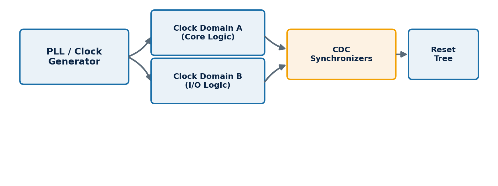
A PLL or clock generator produces one or more base clock frequencies, which are then distributed to different clock domains across the chip – often running at different frequencies for different subsystems. Signals that cross between these domains need synchronization logic to avoid metastability. A reset architecture must ensure every flip-flop starts in a known, safe state, using either synchronous or asynchronous reset strategies (or a mix), consistently applied across the design.
Why It Matters
Clock domain crossing bugs and reset issues are notoriously difficult to catch in simulation and can cause intermittent, hard-to-reproduce failures in silicon. A disciplined, documented clocking and reset plan applied consistently from RTL through implementation avoids entire categories of these bugs.