

What FPGA Debug Involves
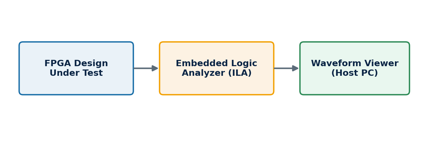
Embedded logic analyzer IP is inserted into the FPGA design alongside the actual logic under test, capturing internal signals as the design runs. These captured waveforms are streamed to a host PC and viewed with standard waveform tools, letting engineers inspect internal chip behavior – the same way they would in simulation – but running at real hardware speed against real software and traffic.
Why It Matters
Some bugs only manifest after millions or billions of clock cycles of realistic operation – timeframes that are completely impractical to reach in simulation but take seconds or minutes on an FPGA prototype. Effective debug infrastructure is what makes this speed advantage actually usable for finding and fixing real bugs.