

Contact
ASIC Architecture Development

Memory Hierarchy Design: Balancing Speed, Capacity, and Cost

No single memory technology is fast, large, and cheap all at once. Memory hierarchy design arranges multiple tiers of storage – from registers to external DRAM – so that the data needed most often sits closest to the compute, while bulk data lives further away.

VIDYUTT July 26, 2026 2 min read
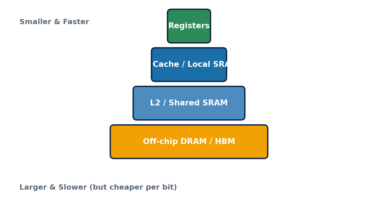
Figure 1: A typical memory hierarchy – small, fast storage near the compute, larger and slower storage further away.

What Memory Hierarchy Design Involves

Registers offer the fastest access but hold only a handful of values. Local caches or SRAM buffers sit close to compute units, trading some capacity for much lower latency and higher bandwidth than off-chip memory. Larger shared caches serve multiple cores or accelerators. Off-chip DRAM or HBM provides the bulk capacity needed for large datasets, at a significant latency and power cost compared to on-chip storage.

Why It Matters

For many workloads – especially AI/ML and signal processing – moving data costs far more energy than computing on it. A well-designed memory hierarchy that maximizes on-chip data reuse can be the difference between a chip that hits its power budget and one that doesn't.

Build your idea into silicon.
From RTL to real, packaged chips through the VACS program.
Start Your Silicon Journey