
What Multi-FPGA Partitioning Involves
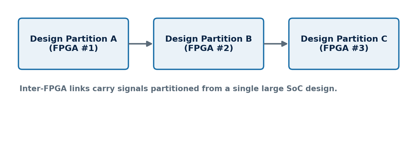
Engineers divide the design into partitions sized to fit available FPGA capacity, while minimizing the number of signals that must cross between partitions – since inter-FPGA connections are far slower and more limited in count than on-chip connections. Specialized partitioning tools help automate this process, but critical-path-aware manual intervention is often needed to keep performance-sensitive logic within a single device where possible.
Why It Matters
A poorly chosen partition can create excessive inter-FPGA signal crossings, severely limiting the achievable prototype clock speed and making software or hardware validation far less representative of the final chip's real-world behavior. Thoughtful partitioning is essential to getting a prototype that's actually useful for meaningful validation.