

What Power Planning & IR Drop Analysis Involve
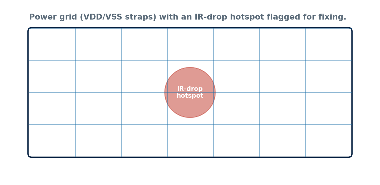
Power planning lays out a grid of metal straps and rings dedicated to carrying VDD and ground (VSS) across the die, sized to handle the expected current demand of the logic beneath them. IR drop analysis then simulates real current draw across the chip to check whether the resulting voltage drop (due to resistance in the metal) stays within acceptable limits everywhere – including under worst-case switching activity that creates temporary current surges.
Why It Matters
Excessive IR drop causes cells to receive less voltage than they were designed and characterized for, which can slow them down unpredictably or cause outright functional failures. IR-drop hotspots – often in high-activity areas like clock buffers or dense logic clusters – need to be identified and fixed with additional power grid reinforcement before tape-out.